
This article will help you determine whether you need a logic level shifter circuit to reliably drive an addressable LED strip with your microcontroller unit (MCU) of choice. And after boring you with an explanation of why a level shifter may be necessary, I’ll provide some recommended options for implementation.
Just to be clear, this article is focused on driving digital “pixel” strips based on popular LED chips such as the WS2811, WS2812b, WS2815, SK6812, and APA102. LED strips based on most of these chips use a single digital data signal (Data Input or Din) from the MCU to control all of the pixels on the strip. Strips based on the APA102 chip use two signals: a serial data input (SDI) and a clock input (CKI). Regardless of the type that you’re using, everything described here applies equally to all of the digital signals from the MCU to the LED strip.
This article only briefly touches on the power and ground connections to the LED strip, but for more on this topic you might want to read the section of this article titled LED Strip Power Injection. If you already understand digital logic concepts and want to quickly figure out if you need a level shifter in your situation, you might want to skip ahead to the MCU Chip Logic Levels section of this article.
Digital Logic Levels
I’m going to dive into details pretty quickly. If you need a refresher on digital logic basics, this tutorial seems pretty good. Let’s start by looking at how two devices (chips) communicate with each other using digital logic, as illustrated below.

In this context, the “driver” is the output circuit of one of the MCU’s general-purpose I/O (GPIO) signals, and the “receiver” is the input circuit of the Din signal for the first chip in the LED strip. The power supply voltage of the MCU chip is represented by VCC(drv) and the power supply voltage of the LED’s logic circuitry is VCC(rcv). Note that these voltage level are not necessarily the same as the power supply voltage applied to the MCU board, or to the LED strip, but we’ll get to that distinction later.
In the diagram above, the MCU firmware has sent a brief logic “high” pulse to the output pin through the driver circuit. Prior to the start of the pulse, the voltage at the driver output is at the logic “low” level, which for real-world circuits is slightly above 0 volts (ground). This output-low voltage is referred to as VOL. At the start of the pulse, the driver output voltage transitions to the output-high level VOH, which is somewhat lower than VCC(drv). The rate at which the driver output rises from VOL to VOH (and later falls back again) depends on several factors:
- The design and capabilities of the driver output circuit, such as how much current it can source (flowing to the receiver circuit) and sink (flowing from the receiver circuit).
- The electrical characteristics of the conductor (wire, PCB traces) between the driver and receiver, especially the amount of parasitic capacitance. Drivers with high current source/sink capabilities are better able to quickly charge and discharge the parasitic capacitance, as needed to achieve fast signal rise and fall times.
- The design of the receiver circuit, although for most LED chips this is a much less significant factor than the first two.
Apart from considerations of the dynamic signal characteristics (e.g. rise and fall times), the key here is to ensure that the receiver will always correctly interpret the static logic levels from the driver (VOL and VOH) under all possible operating conditions, especially conditions that are difficult to predict or control. These variable conditions include:
- Minor variations in the power supply voltages at the driver or receiver caused by transients spikes or droops, temperature changes, or simply a mis-calibrated power supply output.
- Temperature variations that affect the performance of the driver output and receiver input circuits.
- Electrical noise that creates transient voltage spikes (both positive and negative) in the signal between the driver and receiver.
- Manufacturing variations of the driver and receiver chips that affect their electrical performance.

Analyzing the compatibility of the driver and receiver circuits starts with looking at the voltage levels required by the receiver to reliably interpret the logic signal at its input. In the diagram at right, VI is the voltage at the receiver input, which should always be in the range 0v ≤ VI ≤ VCC(rcv).
If VI ≥ VIH(min), the the receiver is “guaranteed” to interpret the input as a high logic level. If VI ≤ VIL(max), the receiver will interpret the input as a low logic level. If the input is between VIL(max) and VIH(min), the output of the receiver is unspecified, so the goal is to avoid this “gray zone” unless the signal is transitioning between low and high levels. The data sheet for every digital logic device contains the specifications for VIH(min) and VIL(max) at the recommended operating conditions (e.g., temperature and VCC ranges).
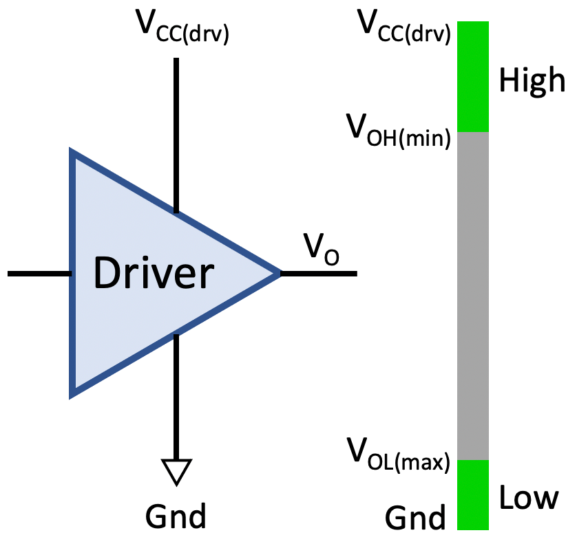
The next step is to look at the voltage levels that will be output by the driver, according to the specifications in the data sheet. As shown at right, VO is the voltage at the driver output, which will always be in the range 0v ≤ VO ≤ VCC(drv).
Under static conditions (after signal level transitions are complete), the data sheet specifies that VO ≥ VOH(min) for a logic high output and VO ≤ VOL(max) for logic low. Another way of saying this is that under the worst-case conditions (within the stated ranges of temperature and VCC), the post-transition output voltage will always be greater than VOH(min) or less than VOL(max). The compatibility of the output signal with the receiver input requirements (for this example) is illustrated below.

The differences (VOH(min) – VIH(min)) and (VIL(max) – VOL(max)) are referred to as “design margins” and should always be positive values. These margins, if large enough, will allow the circuit to operate reliably even in the presence of some of the unpredictable conditions mentioned above, especially noise. The typical design margins for modern CMOS digital logic, using the 74HCT logic family as an example, are:
- Logic high margin = (VOH(min) – VIH(min)) = 4.4v – 2.0v = 2.4v
- Logic low margin = (VIL(max) – VOL(max)) = 0.8v – 0.1v = 0.7v
OK, enough generalities; let’s look at the specifics of MCUs and LED strips.
MCU Chip Logic Levels
Most MCU (processor) chips operate with a power supply voltage of either 3.3v or 5v, and the associated logic levels used by these chips are referred to as “3.3v logic” or “5v logic”. Unfortunately it’s not always immediately obvious what logic levels your MCU uses. That’s because many MCU chips can operate at either 3.3v and 5v, and it’s up to the MCU board designer/manufacturer to decide which voltage to use. For example, an MCU board may require a 5v external power source, but the board design may include a voltage regulator that reduces the voltage from 5v to 3.3v which is supplied to the MCU chip. To confuse matters, some manufacturers offer two different versions of a similarly-named MCU board, one operating at 3.3v and one at 5v. Note that some manufacturers refer to a “3v version” of an MCU, but they really mean 3.3v, which is a standardized supply voltage for CMOS logic.
So you’ll need to dig into the specifications of your MCU board to determine what chip supply voltage is used, and therefore what logic levels apply. The good news is: if your MCU chip uses 5v logic levels, you can bail out now because none of what follows is applicable to your situation. (well, you might want to check out the last couple of sections).
If your MCU uses 3.3v logic levels, you’re going to want to use a logic level shifter circuit to ensure reliable operation. You’ll find plenty of people claiming that their LED project works fine without level shifters, but they’re actually running with inadequate design margins and are just lucky that one particular MCU chip and one particular LED strip usually seem to work correctly at room temperature in the absence of any noise sources. Except during a full moon…
Actually, you could make an argument that chip manufacturers are overly cautious and that the performance will almost always be much better than what is specified in the data sheet. There’s some truth to that, but the problem lies in the word almost. There is no guarantee that a manufacturing process variation might result in them shipping a batch of parts that just barely meets the specification. Even though your design works in the lab, the subsequent copies of your design that get shipped out may not work at all. Customer unhappiness ensues.
If you’re ambitious you can look up the data sheet for your MCU chip for the details of the logic level output voltages, but I’ve done some of the work for you below (assuming a supply voltage of 3.3v)
| MCU Chip | Manufacturer | Output Voltages | Example MCU boards |
| ATmega328P | Microchip Tech. | VOH(min) = 2.3v VOL(max) = 0.5v | Arduino Pro Mini 328 3.3v |
| ESP32 | Espressif Sys. | VOH(min) = 2.64v VOL(max) = 0.33v | Sparkfun ESP32 Thing |
| i.MX RT1060 | NXP | VOH(min) = 3.15v VOL(max) = 0.15v | PJRC Teensy 4.0/4.1 |
There’s quite a bit of variation, with a 0.85v difference between VOH(min) for the “best” chip (i.MX RT1060) and VOH(min) for the “worst” chip (ATmega328P).
LED Chip Logic Levels
Although some addressable LED strips require a 5v power supply and some use a 12v supply, all currently-manufactured LED chips within these strips operate with 5v logic levels. The reason is that the LEDs chips used in 12v strips (such as the WS2815) each contain an internal voltage regulator to provide a 5v supply to the chip’s logic.
There is somewhat less variation in the logic level input voltage specifications for addressable LED chips. Most of the chip types (WS2811, WS2812b, WS2815, SK6812, and APA102) are specified the same, but the latest version (V5) of the WorldSemi WS2812b chip has significantly better specs:
| Most LED chips | WorldSemi WS2812b V5 |
| VIH(min) = 0.7 • VCC = 3.5v VIL(max) = 0.3 • VCC = 1.5v | VIH(min) = 2.7v VIL(max) = 0.7v |
MCU/LED Logic Level Compatibility
Hopefully you’re seeing the problem shaping up here. Regardless of the combination of MCU chip and LED chip used, the design margins are much lower than would be typically recommended. Note that the 74HCT logic design margins previously described would make sense for a driver and receiver that are located on the same circuit board, connected with carefully routed traces, with low-impedance power planes that connect the chips to a common power source. Contrast that with a typical LED project scenario, with the MCU board and LED strip possibly using separate power supplies, and with a long, unshielded cable connecting the two. Settling for lower margins in this scenario doesn’t make for a robust design.
The table below summarizes the design margins for the best and worst MCU/LED combinations.
| MCU Chip | WS2812b Chip | Marginhigh | Marginlow |
| ATmega328P | Pre-V5 | (VOH(min) – VIH(min)) = -1.2v | (VIL(max) – VOL(max)) = 1.0v |
| i.MX RT1060 | V5 | (VOH(min) – VIH(min)) = 0.45v | (VIL(max) – VOL(max)) = 0.55v |
For the graphically-minded, here’s an illustration of the worst-case combination:

Level Shifters to the Rescue
After that long-winded explanation, I’m happy to tell you that there’s a relatively easy fix to the logic level incompatibility between 3.3v MCUs and 5v LED chips: a logic level shifter circuit. Note that these circuits may also be referred to as a “converter” or “translator”, but the idea is the same.
All of the level shifter circuits described in this article are based on integrated circuits (chips) that were designed with this application in mind (among many others). An online search may turn up other level shifter designs based on discrete devices such as MOSFETs, but these designs are unlikely to provide the performance needed to reliably drive addressable LEDs. The issue here is that the serial data protocol used by most LEDs operates at a fairly high frequency (800 KHz is typical). Discrete device-based designs do not have the symmetric, high-current drive capability that allows the data (or clock) signal to be driven both high and low while meeting the maximum rise/fall time specifications for the protocol.
All of the chip-based level shifter designs operate on the same principle: while the shifter chip itself runs on a 5v supply, its input circuits are designed to be compatible with 3.3v logic. The outputs, however, produce voltage levels that are compatible with 5v logic. Simple. The first three shifter chips described below have nearly-identical input/output voltage specifications:
| VIL(max) | VIH(min) | VOL(max) | VOH(min) |
| 0.8v | 2.0v | 0.1v | 4.4v |
As you can see, the input receivers in these chips provide ample margins for interpreting the inputs from the 3.3v MCU chip, while the outputs are driven close to the 5v logic level “rails”, resulting in improved margins for the data signal to the LED chip.
A generic level shifter circuit looks like this:

The sections below describe four similar level shifter designs based on four different chips, each with its own set of minor advantages and disadvantages. With one exception (noted below), all of these can provide reliable operation with any combination of MCU chip and LED chip.
Design #1: 74HCT245

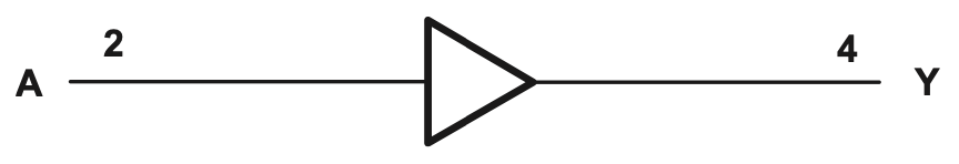
The most common level shifter circuit is based on the 74HCT245 Octal Bus Transceivers with 3-State Outputs. The chip’s internal logic diagram is shown at right. Each of the 8 channels can be used independently to drive up to 8 LED strips. For this circuit, neither the bi-directional capability or the 3-state output capability are used. When the DIR input is connected to VCC (5v) and the OE/ output is connected to Ground, the logic diagram reduces to a set of 8 uni-directional drivers with the inputs on the “A” side and outputs on the “B” side. The driver output circuit uses a symmetric push-pull design that can source or sink up to 6mA (that’s pretty good for driving a long cable to the LED strip).
There are may variants of this chip, and the part number will contain prefixes and suffixes that indicate the manufacturer, the maximum operating temperature range, the reliability screening level, and the package type. It’s available in a 20-pin through-hole package (DIP) for about $0.68 USD in single-unit quantity (example). It’s also available in a surface-mount (SMT) package for as little as $0.49 USD (example).
There is also an “advanced” version of the HCT logic family called AHCT, so this same design can be built using the 74AHCT245 chip (example). AHCT logic is much faster than HCT logic, but that’s not really an advantage in this application (HCT is plenty fast). A real advantage is that AHCT output drivers circuits can source/sink 8mA versus 6mA for HCT. Also note that AHCT applies slew rate controls to the outputs, so that signal ringing won’t be any more of an issue than with HCT logic (see the section below on Dynamic Signal Quality for more details).
If you’re not able to design and build your own circuit board containing a 74HCT245-based level shifter, you may be able to find a pre-built shield/breadboard that you can wire between your MCU board and the LED strip. Here’s one example.
While this design is very cost-effective on a per-channel basis, the disadvantage is that the chip is a bit large if you only need a couple of channels. The other designs below are good options to address that concern.
Design #2: 74HCT125

Another viable design is based on the 74HCT125 Quadruple Bus Buffer Gates with 3-State Outputs. This chip has 4 channels, with each channel having the logic diagram shown at right. With each of the 4 OE/ inputs connected to Ground, each channel can be used as an independent driver with inputs on the “A” side and outputs on the “Y” side. The driver output circuit capabilities are identical to those of the 74HCT245.
The 74HCT125 is available in a 14-pin through-hole DIP for about $0.42 USD (example) and in a SMT package for $0.33 USD (example).
Design #3: 74LV1T34
This design option is based on the 74LV1T34 Single Power Supply Single Buffer GATE CMOS Logic Level Shifter (whew!). It’s a single-channel chip with no control inputs. The driver output circuit is similar to the other chips above, but has an 8mA current source/sink capability for improved dynamic performance.
The 74LC1T34 is only available in a small 5-pin SOT23 (SMT) package, with a cost as low as $0.43 USD (example).
While this option is the least cost-effective on a per-channel basis, this may be the best option for systems that only need one or two channels. The small package provides flexibility in circuit board layout, and the specifications suggest that it may provide better overall performance than the two designs above.
Design #4: TC4427

The final recommended design option is based on the TC4427 1.5A Dual High-Speed Power MOSFET Drivers. Although this chip is intended for completely different applications, it has been proven to work well as an LED strip level shifter/driver. A major advantage is its very high current source/sink capability (1.5A !), allowing it to drive cables up to 30 feet (9 meters) long.
This small 8-pin chips is available in a DIP package (example) for $1.55 USD and an SMT package (example) for $1.20.
While the TC4427 is much more expensive than the other options, it may be a good choice when the MCU will be located a long distance from the LED strip(s). One caveat, though: the TC4427 input-side logic levels are more restrictive than those for the previous three designs:
| VIL(max) | VIH(min) | VOL(max) | VOH(min) |
| 0.8v | 2.4v | 0.025v | 4.98v |
The relatively high spec for VIH(min) means that the TC4427 wouldn’t be a good choice for use with the ATmega328P MCU, which has a VOH(min) spec of only 2.3v, leading to a -0.1v design margin.
Other Design Options?
There are several other level shifter chips/designs floating around that you may be tempted to consider. These designs are all intended for bi-directional logic level translation, such as connecting a 3.3v MCU to a 5v peripheral chip via a bi-directional I2C bus. These chips are designed to drive relatively short circuit board traces at lower speeds than used by the LED serial protocols. While these designs can be adapted for unidirectional applications, there is ample evidence that they do not provide reliable operation in LED applications with long-ish cables.
Some specific chips that fall into this category (i.e., the category to be avoided) are the TXB0108, TXS0102, and PCA9306.

Oh, wait – one more! You may have seen a uni-directional design based on the SN74LVC2G07 Dual Buffer and Driver With Open-Drain Outputs. In this design (right), the chip runs on a 3.3v supply, but relies on a pull-up resistor to achieve the necessary VOH level at the LED chip. While this will work in some situations, the asymmetric output circuit will result in very slow rise times that significantly distort the signal with a longer cable run to the LED strip.
Dynamic Signal Quality
The sections above have described how a symmetric (push/pull) driver output circuit with high current source/sink capability can improve dynamic signal quality by reducing signal transition rise and fall times. But sometimes too much of a good thing can cause other problems that must be mitigated. Very fast rise/fall signals from the driver may cause voltage oscillations (called ringing) at the receiver end of the cable. If these high-frequency voltage swings are are large enough, they may cause unintended logic level changes and corrupt the serial data.
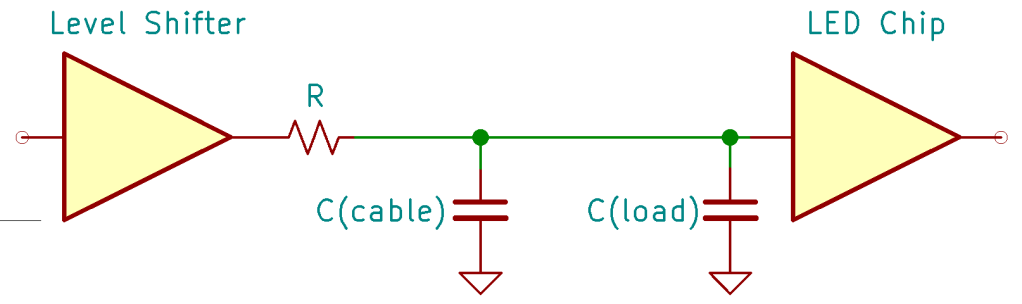
The most common approach to mitigate this issue is to add a small resistor (R) in series with the the signal, between the output of the level shifter and the LED strip input (Din), as illustrated below:
There is considerable confusion and disagreement on the correct placement and value of this series resistor, and hopefully this discussion will clear things up a bit.
As mentioned previously, the interface cable has parasitic capacitance Ccable. Also, the LED chip’s receiver input circuit has load capacitance Cload. The combination of the resistor and the two capacitances form a low-pass R-C filter circuit that effectively slows down the signal rise and fall transitions. Given that the capacitance values are fixed, the resistor value R can be selected to eliminate signal ringing (transitions too fast) while also avoiding excessive signal distortion (too slow).
Another effect of the resistor is more complicated. High slew-rate (fast transitioning) signals can cause voltage spikes to be reflected from the receiver back toward the driver. With the right value, the resistor can partially damp out the signal reflections.
For both of these effects to work, the resistor must be located at the driver side of the cable. Some sources state that the resistor should be located close to the LED chip receiver, but there is no known evidence to support this.
Determining the correct resistor value depends on the specific type of driver (level shifter) used, as well as the characteristic impedance of the cable. An analytic approach to selecting the resistor value is well beyond the scope of this article (i.e., way too complicated!). A more practical approach is to experiment with different resistor values while observing the signal quality at the receiver end with an oscilloscope. Based on anecdotal evidence, resistor values between 33Ω and 220Ω appear to provide good results.
A side-benefit of the the series resistor is that it provides some degree of protection for the driver circuit in the event of some malfunction or mishap involving the LED strip. One possible scenario is the occurrence of a short circuit between the LED strip power supply (5v or 12v) and the Din signal. When the driver attempts to drive the signal low, a low-resistance path is created from the power supply to Ground through driver circuit. A low-value series resistor will still allow a large current flow through the driver, likely well beyond its recommended operating specification, but it could prevent the driver from being permanently damaged.
Wrap Up
Hopefully this article has answered all of your questions about what a logic level shifter circuit does, and why it might be necessary for your new LED lighting project. One less thing to worry about!

This is the dictionary definition of “A Valuable Resource”.
Hundreds, if not thousands, of people need to bookmark this page, or print it to pdf and keep it in a safe place. I will do both.
Well done.
LikeLiked by 1 person
really excellent review, appreciate the time it took to write and share this!
LikeLiked by 1 person
Thanks for the feedback!
LikeLike
In the example sketch shouldn’t the bypass cap be in the VCC line?
LikeLike
Sorry, I haven’t been able to figure out which diagram (sketch?) you’re referring to.
LikeLike
Normally I don’t create any comments, but here I really need to make an exception… This is by far the best article regarding level shifting (and technical blog posts in general) I have read in years! – I only wanted to look up a good shifter working for my SK6812, but this article is enlightening and stuffed with so much useful information…
Thanks a lot for this masterpiece.
Greetings from Germany
j54j6
LikeLike
Thank you very much for your kind comments! I really enjoy getting confirmation that my articles have been helpful.
Greetings from Reno, Nevada, USA!
-Keith
LikeLike
I agree with the other comments; a verry well written and usefull article. Thank you for that.
One question, and apologies in advance for the nood-question: if i were to use a TC4427 for shifting, since it can source 1,5A, would i need to use a 1,5*5=7,5Watt (P=U*I) resistor in series for data? Or should i calculate the power rating for a digital signal in another way?
LikeLike
Paul,
Sorry for the delayed response: I’ve been at Burning Man and just got back to Reno at sunrise this morning. No need to apologize. That’s an excellent question! So, the high current drive capability of the TC4427 is intended to quickly charge (turn on) and discharge (turn off) the gate of an external MOSFET with ~1000pF capacitance. When using this chip to drive the input of an addressable LED input (at then end of a long cable), the high-current capability is used to quickly charge/discharge the parasitic capacitance of the long cable. The capacitance of the data signal in a typical 3-wire LED cable isn’t really easy to calculate, but let’s assume it’s < 1000 pF for a 5m cable. In that case, the high-current condition only occurs during the < 30ns rise/fall time of the 800 KHz data signal. So the duty cycle of the high-current condition is only 2 * (30ns / 1.25uS) = 2.4%. If a 33Ω series resistor is used to dampen transient spikes, the AVERAGE power consumption will be at most (1.5A)^2 * 33 * 0.024 = 1.8W. But that assumes that the TC4427 will source/sink the full 1.5A. That probably won't happen due to the 33Ω resistor and the DC resistance of the long cable. So in reality the average power consumption will probably be much lower. Without a lot more analysis, the easiest approach would be to test the circuit with different resistor values and power ratings. I'm guessing it will be possible to get away with a fairly low-power resistor, maybe 1/4W or even 1/10W. I think by now you've picked up on the fact that resistors are more sensitive to average power than instantaneous power; it's all about sustained temperature.
Whew! That question was harder than I thought. Good luck!
LikeLike
No worries about any delay. Thank you so much for the elaborate answer. I hope you had a wonderfull time at the festival.
So for the powerrating i have to go about the average, not the verry short peaks. Got it! But still. I’m yet to figure out how to calculate the needed resistor value. Several online articles tell a different story and online calculators give different results. So using the 220 ohm mentioned in your article as a maximum i would possibly need to use up to 1,5^2 * 220 * 0,024 = 11,9 watt power rated resistors? That are quite heavy resistors to put in a driver-circuit. Or am i missing something here? How can i factor in the cable’s resistance?
Thank you in advance.
LikeLike
Hello,
Thank you for this wonderfully detailed article.
I have ordered a few SK6812 LED strips that I plan to drive with several ESP32 controllers (WT32-ETH01).
If I keep the data line from the controller to the first LED short to minimise voltage drop, I guess I don’t need a level shifter because I am within the tolerance of the LED driver. The problem occurs if the data line to the first LED is too long. But in this case, instead of using a level shifter to boost power to 5V, can’t I use a single pixel close to the controller that basically acts like a level shifter? I can setup WLED to ignore this pixel in order to keep it switched off.
Is this solution viable?
LikeLike
That’s a great question. The answer depends on whether you want something that will “probably work most of the time” or something that will “always work correctly under all conditions”. The first answer is often chosen by hobbyists that are designing a lighting system for personal use, because it’s cheaper, easier, and “good enough”. On the other hand, an engineer that’s designing lighting for commercial use will carefully analyze the component specifications, and choose a design that works under the worst-case combination of conditions, such as temperature, supply voltage, external noise sources, cable lengths, and component manufacturing variations. Definitely more work and more cost, but that’s why modern electronic products are generally very reliable.
So here’s the issue: The last time I checked an ESP32 data sheet (specs might vary by specific version), the Voh(min) spec was 2.64V. for a chip using a 3.3V supply voltage. That means that a logic “high” output signal is only guaranteed to be 2.64V. It could be higher, and usually is, but isn’t certain to be under all conditions. The SK6812 LED chip, on the other hand, has a Vih spec of 3.4V. That is, an input data signal of at least 3.4V is required to guarantee that the chip interprets the signal as a logic “1” instead of “0”. That means that an ESP32 output and SK6812 input are not guaranteed to be compatible (work reliably) regardless of how short the interconnect cable is.
Certainly, many people have been successful using the “sacrificial pixel” method that you described. But that’s only because the specific ESP32 chip and SK6812 LED chip they’re using are exceeding their specifications. And that’s probably OK if you’re only building one system for your own use. But a reputable company would never sell a product that was designed like that.
One more thing: The length of the data cable doesn’t result in significant “voltage drop”, since very little current flows through the data wire. The issue with long cables is that the signal voltage can be affected by internal and external noise sources that cause voltage spike to be superimposed on the signal. An external noise source could be a nearby motor or relay. Internally-generated noise is caused by reflections of the data signal edges/transitions, and that’s the most common cause of flickering and erratic operation in addreessable LED systems.
For more information on issues caused by long cables, see my article “Wiring Design for Addressable LED Strips”:
Sorry for the super-nerdy response, but that’s the way I roll…
LikeLike